
Concepts: Energy bands and the classification of solids
Semiconductor Electronics: Materials, Devices and Simple Circuits19 min readLesson 2 of 7
2.1 From valves to semiconductors
Electronic circuits are built from devices in which the flow of electrons can be controlled. Before the transistor arrived in 1948, that control came from vacuum tubes, also called valves. A vacuum diode had two electrodes, a cathode and an anode or plate. The triode added a grid, and the tetrode and pentode added more electrodes. In all of them the electrons came from a heated cathode and travelled through vacuum, controlled by the voltages on the electrodes. The vacuum was essential: air molecules would otherwise drain the electrons of energy in collisions.
These devices are bulky, need high power and high voltages of the order of a hundred volts, and have limited life and reliability. Semiconductors changed that. From the 1930s it was realised that the number and direction of charge carriers in a semiconductor can be controlled by simple excitations such as light, heat or a small applied voltage. In a semiconductor the supply and flow of carriers happen inside the solid itself, with no heated cathode and no evacuated space. The devices are small, run on low voltage and low power, and last a long time. Even the cathode ray tubes of older televisions are now replaced by flat panels with solid state electronics.
2.2 Classifying solids by resistivity
Solids divide into three broad groups by their electrical behaviour. Metals have very low resistivity, roughly 10 to the -2 down to 10 to the -8 ohm metre. Semiconductors lie in the middle, roughly 10 to the -5 up to 10 to the 6 ohm metre. Insulators have very high resistivity, from about 10 to the 11 ohm metre upwards. These ranges show magnitudes rather than sharp borders, so resistivity alone is not the whole story, but it is a useful first classification.
Semiconductors themselves come in types. Elemental semiconductors are silicon and germanium. Compound semiconductors include inorganic materials such as cadmium sulphide, gallium arsenide, cadmium selenide and indium phosphide, organic materials such as anthracene and doped phthalocyanines, and conducting organic polymers such as polypyrrole, polyaniline and polythiophene. Most practical devices use silicon or germanium or the inorganic compounds; the notes here stay with the elemental ones, because the concepts carry over.
2.3 Why the band picture is needed
In an isolated atom the energy of an electron is decided by its orbit. When atoms pack into a crystal they sit close enough for outer orbits to overlap, and the motion of an electron becomes very different. Each electron sees a slightly different pattern of surrounding charges, so each has a slightly different energy. The result is a band of almost continuous energy levels rather than a single sharp level.
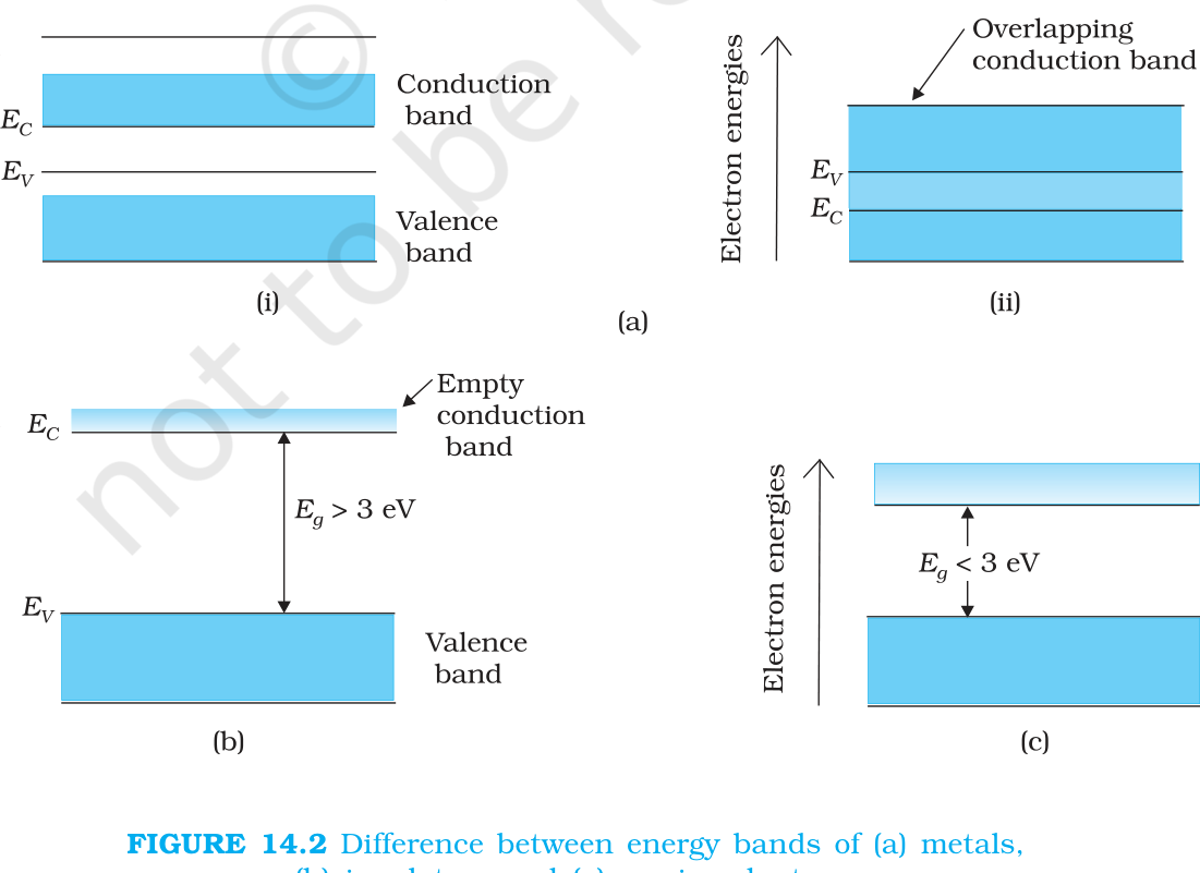
Valence electrons occupy the valence band; the band lying above it is the conduction band. With no external energy the valence band is full and the conduction band is empty. When the bottom of the conduction band sits below the top of the valence band the two overlap, electrons move freely, and the solid conducts. Metals look like this (Figure 14.2a). If the bands are separated by a gap, electrons need energy to cross it. A large gap makes an insulator (Figure 14.2b). A small gap makes a semiconductor, because at room temperature a few electrons can pick up enough thermal energy to cross over (Figure 14.2c).
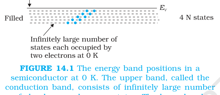
For a silicon crystal of N atoms the outer shell holds four electrons per atom, so 4N valence electrons occupy states in a band that can take 8N electrons. At the interatomic spacing of silicon and germanium this band splits into two: a lower band completely filled by the 4N electrons at absolute zero, which is the valence band, and an upper band with 4N states that is completely empty, the conduction band (Figure 14.1). The bottom of the conduction band is labelled E C, the top of the valence band E V, and the gap between them is the energy gap E g. An electron that crosses the gap leaves a vacancy in the valence band, and that vacancy behaves like a positive charge, which is the hole. Both the electron in the conduction band and the hole in the valence band take part in conduction.
2.4 What the overlap actually means
When the bands overlap, there is no gap for an electron to jump, so a metal needs no excitation at all to conduct. In a semiconductor the gap is small enough that room temperature supplies the few hundredths of an electron volt needed by a small fraction of electrons, while the rest stay in the valence band. The picture also explains why the number of carriers in a pure semiconductor is so much smaller than in a metal: only the tail of the thermal energy distribution reaches across the gap.