
Concepts: Intrinsic semiconductors
Semiconductor Electronics: Materials, Devices and Simple Circuits18 min readLesson 3 of 7
3.1 The crystal and its bonds
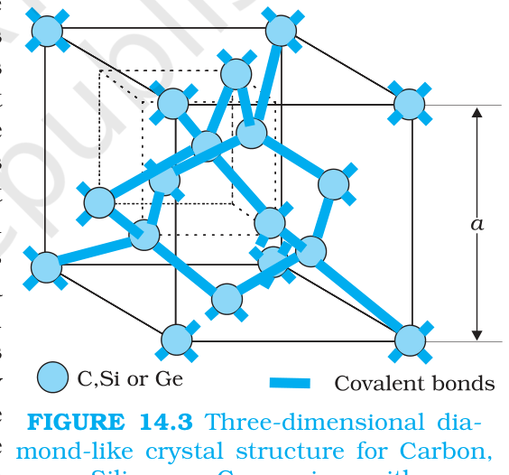
Silicon and germanium crystallise in a diamond-like lattice (Figure 14.3). Each atom has four nearest neighbours. Both elements have four valence electrons, and in the crystal every atom shares one of its valence electrons with each neighbour, and takes a share of one from each. These electron pairs form covalent bonds that hold the lattice together.
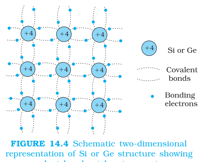
At low temperatures all bonds are intact, and Figure 14.4 shows the arrangement in two dimensions, with the inner cores marked and the shared electrons implied. This is the ideal picture, and it describes the material near absolute zero, where there are no free carriers.
3.2 Thermal generation of carriers
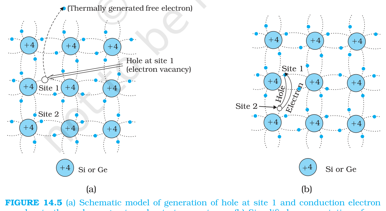
As the temperature rises, thermal energy becomes available to the electrons. A few bonds break, and the electron that leaves becomes free to move through the crystal. The place it left behind is a vacancy in a bond, and that vacancy carries an effective positive charge of the same size as the electron's negative charge. This is a hole. The hole behaves like a free particle with positive charge, and it can move: an electron from a neighbouring bond can jump into the empty bond, which shifts the vacancy to the neighbouring site. The apparent motion of the hole is therefore the real motion of bound electrons filling vacancies one after another (Figure 14.5).
So there are two kinds of carriers in a semiconductor. The free electron moves in the conduction band and carries an electron current I e. The hole moves in the valence band and carries a hole current I h. Under an applied field the electrons drift towards the positive terminal and the holes towards the negative terminal, and the total current is the sum I = I e + I h. That a semiconductor conducts with two carrier types is what separates it from a metal, where only electrons carry current.
3.3 Generation and recombination
Free carriers are created by thermal generation, and they are destroyed by recombination, when an electron meets a hole. At equilibrium the rate of generation equals the rate of recombination, so the carrier concentrations stay steady. The number of free electrons equals the number of holes, because each broken bond creates one of each:
n e = n h = n i
where n i is the intrinsic carrier concentration, a property of the material and its temperature. For silicon at room temperature n i is of the order of 10 to the 16 per cubic metre, and for germanium it is higher.
3.4 Band picture and temperature dependence
At absolute zero an intrinsic semiconductor behaves like an insulator: the valence band is full, the conduction band is empty, and there is no conduction (Figure 14.6a). At any temperature above zero some electrons are thermally excited across the gap and partially occupy the conduction band, leaving an equal number of holes in the valence band (Figure 14.6b). Because the number of carriers is set by the fraction of electrons with enough thermal energy to cross E g, the conductivity rises with temperature. This is the opposite of a metal, where resistance rises with temperature because the lattice scatters electrons more strongly.
The size of the gap decides how strong the effect is. Carbon, silicon and germanium have the same lattice structure and four valence electrons, but their gaps are about 5.4 eV, 1.1 eV and 0.72 eV respectively. At a given temperature far more electrons can cross the smallest gap, so germanium conducts better than silicon, and diamond behaves as an insulator (Figure 14.6).
3.5 Reading the carrier numbers
The intrinsic concentration is small but far from zero. For silicon at room temperature n i is of the order of 10 to the 16 per cubic metre, while the crystal itself holds around 10 to the 28 atoms per cubic metre. So roughly one in a thousand billion bonds is broken at any instant, and that tiny fraction is enough to give a measurable conductivity. When the material is doped, the dopant numbers are chosen in parts per million, which lands the carrier count many orders above the intrinsic value.
The hole is a bookkeeping device with real consequences. A hole near the top of the valence band behaves like a particle with positive charge and a mass of its own, and it responds to electric and magnetic fields just as an electron does, only in the opposite direction. When a question asks why a semiconductor is called a two-carrier conductor, this is the answer: drift of electrons in the conduction band and drift of holes in the valence band add up to the observed current.