
Concepts: Extrinsic semiconductors and the p-n junction
Semiconductor Electronics: Materials, Devices and Simple Circuits20 min readLesson 4 of 7
4.1 Why dope
A pure semiconductor conducts only weakly at room temperature, too weakly for useful devices. Adding a tiny amount of a suitable impurity, a few parts per million, raises the conductivity manifold. The deliberate addition is called doping, the impurity is the dopant, and the result is an extrinsic or impurity semiconductor. The dopant must fit the lattice, so its atoms have to be close in size to the semiconductor atoms. For tetravalent silicon or germanium there are two families of dopants: pentavalent atoms such as arsenic, antimony and phosphorus, and trivalent atoms such as indium, boron and aluminium.
4.2 n-type material
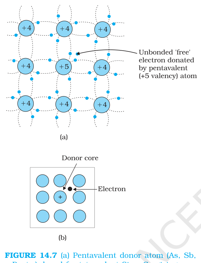
Insert a pentavalent atom in place of a silicon atom (Figure 14.7). Four of its electrons enter bonds with the four neighbours; the fifth has no bond waiting for it. That fifth electron sits only weakly bound to its parent atom, because the four bonding electrons largely screen the nucleus. The energy needed to set it free is very small, about 0.01 eV in germanium and about 0.05 eV in silicon, compared with the roughly 0.72 eV or 1.1 eV needed to cross the full band gap. So at room temperature the extra electron is free to conduct.
A pentavalent dopant therefore donates an electron, and it is called a donor. The number of electrons supplied depends on the doping level and hardly on temperature, while the intrinsic electron-hole pairs still grow slowly with temperature. The donor electrons far outnumber the holes, but the recombination rate rises with the extra electrons, so the hole number falls further. So n e far exceeds n h, electrons become the majority carriers, holes the minority, and the material is n-type.
4.3 p-type material
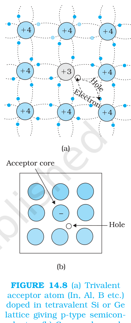
Now put in a trivalent atom (Figure 14.8). It has one valence electron fewer than silicon, so it forms bonds with three neighbours and has nothing to offer the fourth. The fourth bond therefore contains a vacancy, a hole. A neighbouring electron can jump into that vacancy, leaving a hole at its own site, so the hole is free to move under a field. The trivalent atom becomes effectively negatively charged when it accepts the fourth electron, and it is called an acceptor. One acceptor gives one hole, so holes become the majority carriers and electrons the minority carriers. This is p-type material.
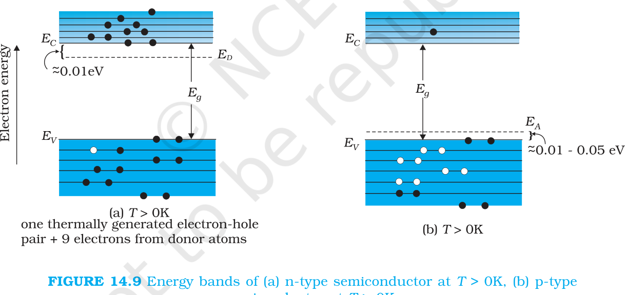
Doping also puts new levels into the band picture. In n-type silicon a donor level E D sits just below the conduction band edge E C, so electrons from it enter the conduction band with very little energy (Figure 14.9a). In p-type material an acceptor level E A sits just above the valence band edge E V, and electrons from the valence band rise to it easily, which is the same as holes appearing in the valence band (Figure 14.9b). In thermal equilibrium the carrier product is fixed: n e n h = n i squared. The material stays neutral because the charge of the extra carriers is balanced by the ionised dopant cores.
4.4 Building the p-n junction
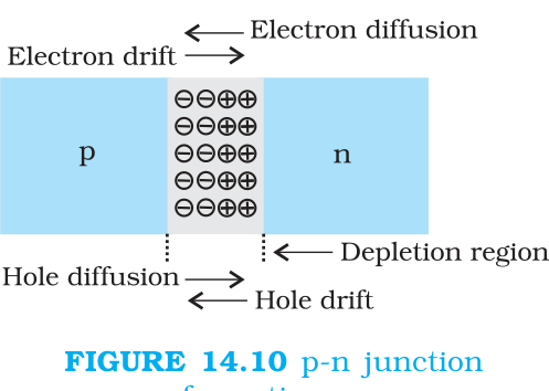
To make a junction, one region of a wafer is doped p-type and the neighbouring region n-type (Figure 14.10). Two processes act at the boundary. The first is diffusion: electrons are far more numerous on the n-side, so they diffuse across to the p-side, and holes are far more numerous on the p-side, so they diffuse to the n-side. When an electron leaves the n-side it leaves behind a fixed positive donor ion, and when a hole leaves the p-side it leaves behind a fixed negative acceptor ion. The two space-charge layers build up on either side of the junction and together make the depletion region, roughly a tenth of a micrometre thick and almost free of mobile carriers.
The second process is drift. The space charge sets up an electric field pointing from the positive n-side to the negative p-side. This field pushes electrons back towards the n-side and holes back towards the p-side, so a drift current runs opposite to the diffusion current. At first diffusion is large and drift small, but as the space charge grows the field and the drift current grow too. Equilibrium arrives when the two currents are equal, and the junction then has no net current.
The charge separation also creates a potential difference across the junction, with the n-side positive with respect to the p-side. This potential opposes further movement of carriers, which is why it is called the barrier potential. Under forward bias the external voltage opposes the barrier and lowers it to V0 - V; under reverse bias the external voltage adds to the barrier and raises it to V0 + V while widening the depletion region.
The balancing rule is easy to remember: the product of the two carrier concentrations stays fixed at n i squared, so making one type plentiful forces the other type down. That is why doping an intrinsic sample of holes with a donor reduces the hole number at the same time as it raises the electron number.